Solder mask
You can help expand this article with text translated from the corresponding article in German. (June 2018) Click [show] for important translation instructions.
|

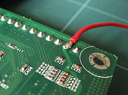
Solder mask, solder stop mask or solder resist is a thin lacquer-like layer of polymer that is usually applied to the copper traces of a printed circuit board (PCB) for protection against oxidation and to prevent solder bridges from forming between closely spaced solder pads. Soldermask[2] is a printed circuit board (PCB) manufacturing process that uses a chemical or thermosetting resin to coat a thin film on a circuit board, which can effectively form a layer of reliable protection to avoid unwanted short-circuiting and leakage of the circuit board, and to improve the reliability and electrical performance of the circuit board. A solder bridge is an unintended electrical connection between two conductors by means of a small blob of solder. PCBs use solder masks to prevent this from happening. Solder mask is not always used for hand soldered assemblies, but is essential for mass-produced boards that are soldered automatically using reflow or wave soldering techniques. Once applied, openings must be made in the solder mask wherever components are soldered, which is accomplished using photolithography.[1] Solder mask is traditionally green, but is also available in many other colors.[2]
Solder mask comes in different media depending upon the demands of the application. The lowest-cost solder mask is epoxy liquid that is silkscreened through the pattern onto the PCB. Other types are the liquid photoimageable solder mask (LPSM or LPI) inks and dry-film photoimageable solder mask (DFSM). LPSM can be silkscreened or sprayed on the PCB, exposed to the pattern and developed to provide openings in the pattern for parts to be soldered to the copper pads. DFSM is vacuum-laminated on the PCB then exposed and developed. All three processes typically go through a thermal cure of some type after the pattern is defined although LPI solder masks are also available in ultraviolet (UV) cure.
The solder stop layer on a flexible board is also called coverlay or coverfilm.[3]
In electronic design automation, the solder mask is treated as part of the layer stack of the printed circuit board, and is described in individual Gerber files for the top and bottom side of the PCB like any other layer (such as the copper and silk-screen layers).[4] Typical names for these layers include tStop/bStop aka STC/STS[5][nb 1] or TSM/BSM (EAGLE), F.Mask/B.Mask (KiCad), StopTop/StopBot (TARGET), maskTop/maskBottom (Fritzing), SMT/SMB (OrCAD), MT.PHO/MB.PHO (PADS), LSMVS/LSMRS (WEdirekt)[6] or GTS/GBS (Gerber and many others[7]).
Notes
[edit]- ^ The letters 'C' and 'S' in EAGLE's old Gerber filename extensions
.STC/.STSfor the top and bottom solder stop mask layers have their origin in times when printed circuit boards were typically equipped with components populated on one side of the board only, the so called "component side" (top) versus the opposite "solder side" (bottom) where these components were soldered (at least in the case of through-hole components).
References
[edit]- ^ Mitzner, Kraig (2009). Complete PCB Design Using OrCAD Capture and PCB Editor. Burlington, Massachusetts, USA: Elsevier, Inc. pp. 9–10. ISBN 978-0-7506-8971-7.
- ^ Williams, Jody (2005-03-01). "Soldermask: it's not just green anymore whether it's to identify revision changes or to look trendy in a see-through box, soldermask is taking on a rainbow of colors. But your processes will have to change with the hues". UP Media Group, Inc. Archived from the original on 2022-08-29. Retrieved 2015-11-14.
- ^ Tome, Paul (2014-03-14). "What is a Flexible Circuit Coverlay?". epec. Archived from the original on 2022-11-14. Retrieved 2022-11-14.
- ^ Wright, Allan (2007-04-14). "FreePCB User Guide" (PDF). 1.4. Archived (PDF) from the original on 2018-06-17. Retrieved 2018-06-17.
- ^ "Preparing the Manufacturing Data: Gerber Files for Photoplotters with Variable Aperture Wheels". EAGLE - Easily Applicable Graphics Layout Editor - Manual - Version 3.55 and later (PDF) (2 ed.). Delray Beach, Florida, USA: CadSoft Computer, Inc. 1999. pp. 88–90 [89]. Archived (PDF) from the original on 2022-08-30. Retrieved 2022-08-30.
- ^ "Lagenbezeichnungen" [Layer designators]. WEdirekt (in German). Rot am See, Germany: Würth Elektronik GmbH & Co. KG. 2020. Archived from the original on 2022-08-29. Retrieved 2022-08-29. [1]
- ^ "Gerber Output Options" (PDF). 1.3. Altium Limited. 2011-07-27 [2008-03-26, 2005-12-05]. Archived (PDF) from the original on 2022-08-29. Retrieved 2022-08-29.
Further reading
[edit]- Zühlke, Karin (2017-12-12). "Forschungsallianz Fela und Würth - "s.mask" - der erste Schritte zur digitalen Leiterplatte". Elektroniknet.de (in German). Markt & Technik. Archived from the original on 2018-06-17.
